From R&D to Product Development to Manufacturing to Field Testing, BrightSpot can provide you with customized defect imaging solutions for Perovskite and Tandem cell/panel architectures.
BrightSpot was very responsive to our customization needs for an EL/PL system to image our Perovskite cells and mini-modules. The image quality is excellent, and the system is heavily used to provide critical feedback for our R&D efforts.
– John Iannelli, President & Founder Caelux
The highest resolution images, from mm² to m²
BrightSpot utilizes a variety of camera and lens combinations to enable high-resolution imaging over a wide range of device sizes. Even when imaging areas wider than 1 meter, fine features smaller than 0.5 mm can easily be seen. We offer large-area LED illumination at intensities up to 1 sun to capture photoluminescence images of full panels.
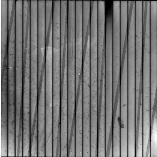
Perovskite EL Image
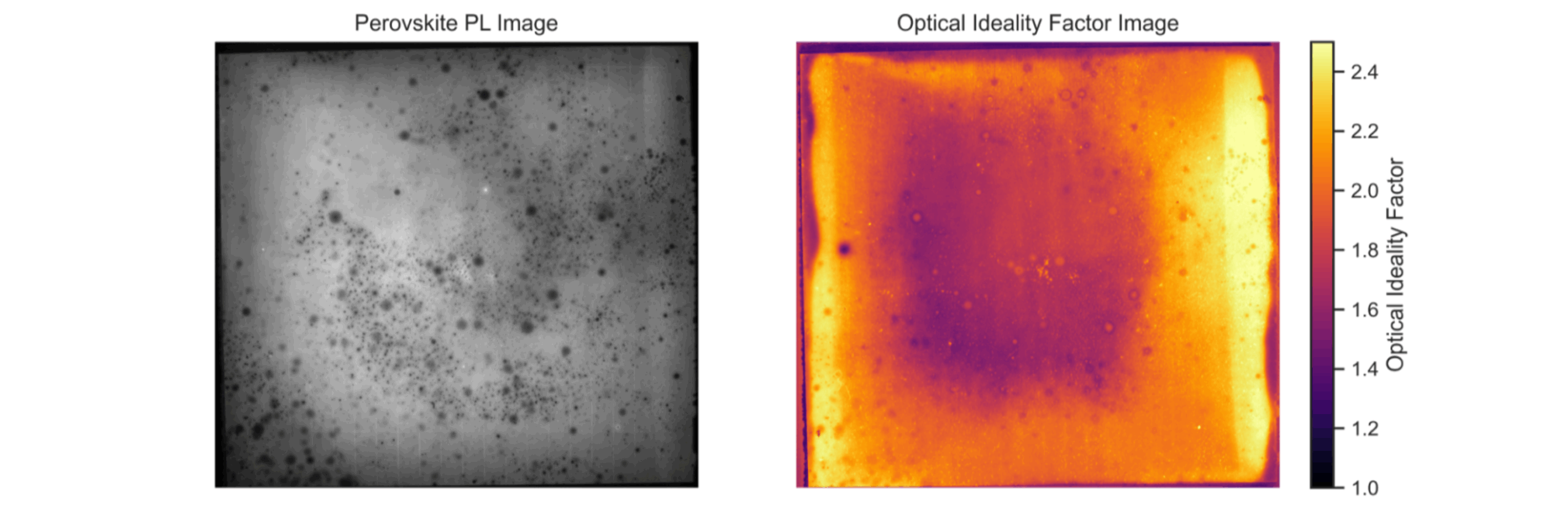
Perovskite PL Image
Standard and Customized Imaging Systems
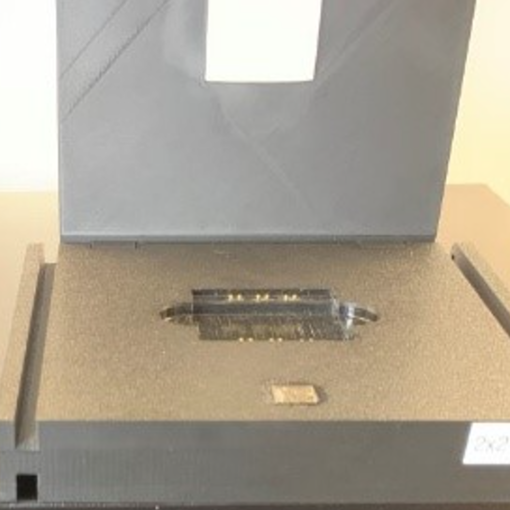
Imaging systems for Perovskite cells/panels range from our standard CellSpot and PanEL-Spot products, to customized system configurations tailored to your specific testing needs.
Available components include:
Large-area cell busbar-probing chuck
Filter Wheel for IMPEL-controlled selection of camera filters
Dual-color PL Light Sources for imaging of top and bottom cells
Customized EL chuck for multiplexed probing of an array of cells
Spectrometer for spot bandgap measurement
How good are your edge and junction box seals?
Perovskites are highly sensitive to degradation from moisture and air ingress from the panel edges and junction box penetrations. BrightSpot’s UV Fluorescence technology has been demonstrated to detect such sealing failures in glass/glass panel construction. UVF should be a standard product development tool to help develop durable Perovskite panels.
Your Needs Covered
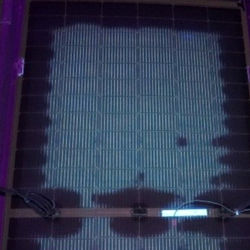
UVF Panel with Sealing Problems
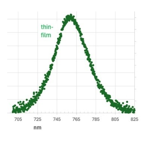
Spectral PL Curve
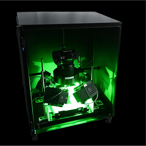
CellSpot with 4x Green Lamps
Chuck for array of small cells
Not just pretty pictures
IMPEL’s automated recipe feature can capture a series of images at different light intensities and/or electrical biases. BrightSpot’s advanced algorithms can analyze these images to create figure of merit maps of important device parameters such as Ideality factor, Rs, iVoc, and PCE.
IMPEL’s automated recipe feature can capture a series of images at different light intensities and/or electrical biases. BrightSpots advanced algorithms can analyze these images to create figure of merit maps of important device parameters such as Ideality factor, Rs, iVoc, and PCE.
Quality control after each fabrication step
Non-contact PL imaging should be performed after each critical step in device fabrication: after Perovskite deposition, after transport layer deposition, and after device completion. Imaging after each step facilitates not only process step optimization, but also statistical process control in manufacturing.
Measure device stability over time
Multi-step recipes in IMPEL enable automatic capture of images over time as devices degrade while exposed to illumination, electrical bias, and other stress factors.
Your Reasearch and Development Partner
As perovskite and tandem (multi-junction) solar cells move from research to early manufacturing, non-contact inspection becomes critical. BrightSpot’s EL and PL systems offer powerful, safe imaging tools for visualizing subcell performance, material defects, and layer consistency across new architectures.
BrightSpot offers customized imaging systems for factory line and robotic integration, offline testing, varied panel orientation and shape, and tight working distance constraints.
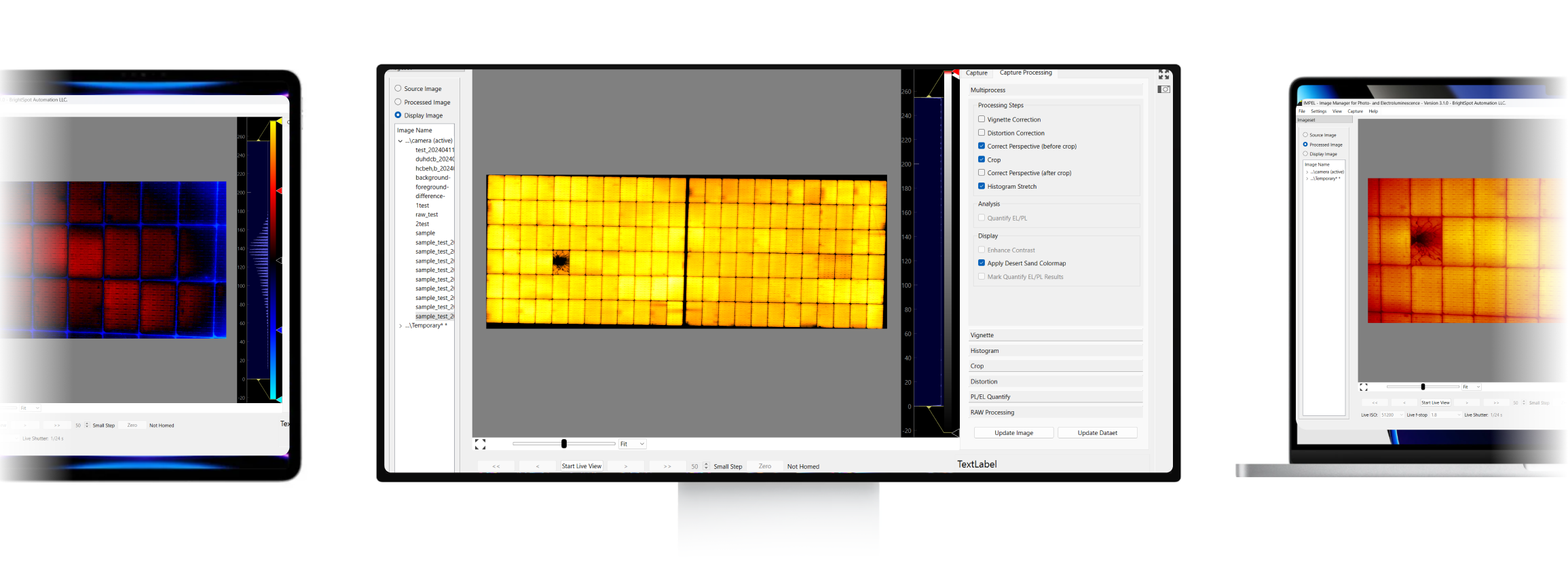
IMPEL is the unified control platform for BrightSpot imaging systems, enabling seamless coordination of the camera, light sources, and power supplies. From a single interface, users can adjust exposure settings, trigger PL or EL sequences, and save all control and post-processing parameters in a convenient “Recipe” format.
Enterprise System Integration
Our software engineering team will customize IMPEL to integrate with your upstream/downstream automation equipment and to save data in a desired location and format.
Report
Built-in image processing tools help users enhance contrast to highlight defects and visualize subtle variations in cell or panel quality.
decades of experience and hundreds of customers
Companies
0
Countries
0
Years
0
Our Latest Publications
The latest publications and technical outputs from BrightSpot Automation
BrightSpot is Exhibiting at the NABCEP CE Conference